


NEO Semiconductor has expanded its 3D X-DRAM concept with new variants aimed at improving retention time, density, and power efficiency. By modifying its original one-transistor, zero-capacitor (1T0C) design to include either a capacitor (1T1C) or additional transistors (3T0C), the company is pushing toward denser, faster, and more energy-efficient DRAM structures that align with 2D DRAM scaling roadmaps.
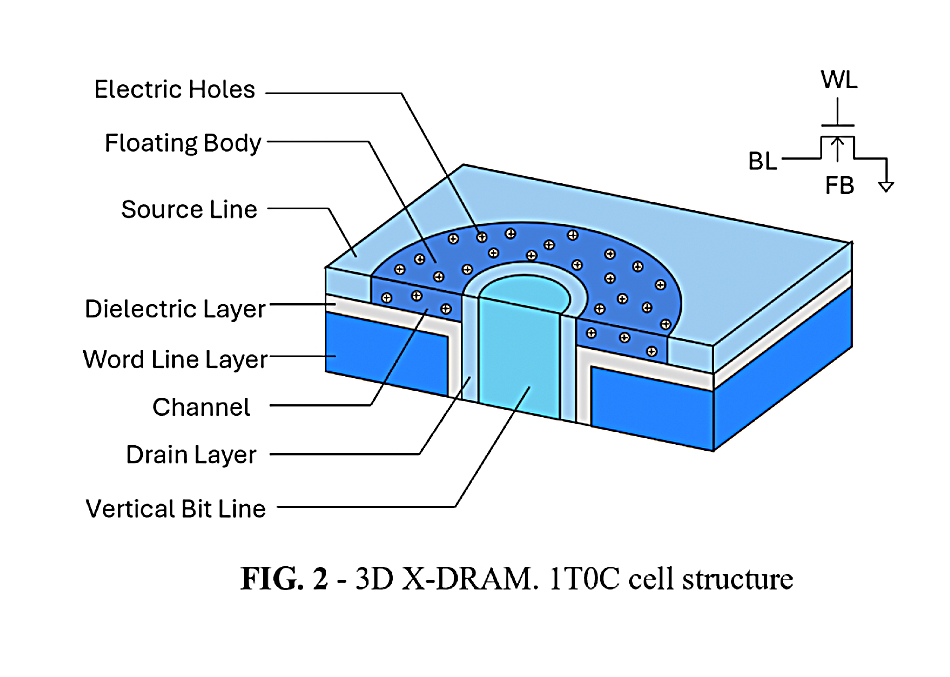
A recently published NEO white paper details the architecture and design choices behind its updated memory cells. The original 1T0C design uses floating body cell technology while the 1T1C development uses an Indium Gallium Zinc Oxide (IGZO) transistor channel. An N+ polysilicon capacitor plate facilitates effective electron storage in the IGZO layer.
The overall 1T1C cell structure looks like this:

The left-hand diagram shows a top word line in place while it has been removed in the right-hand diagram to show the underlying components. NEO says: “The IGZO layer is coupled to a metal word line layer, which acts as the transistor gate. The drain of the IGZO layer connects to a vertical bit line made of materials. A thin high-k dielectric layer, serving as a capacitor, is formed along the cylindrical sidewall on the source side of the transistor between the IGZO channel and a capacitor plate layer. The capacitor plate, composed of conductors such as N+ polysilicon, is biased at VDD to facilitate effective electron storage in the N-type IGZO layer.”
This configuration can achieve a greater than 450 second retention time, meaning cell refreshes are needed less often, and up to 128 layers.
By adding 5nm-thick spacer components between the vertical bit lines and the word line layers, NEO reduces parasitic bit line capacitance so that more than 512 layers can be stacked, increasing device capacity.
There are other 1T1C variants, such as one with a conductor plate, and another that eliminates the insulator between the vertical bit line and the IGZO layer. The 3T0C design looks like this:

It incorporates two IGZO layers for enhanced performance. This design relies on current sensing and is “particularly well-suited for in-memory computing and artificial intelligence (AI) applications, where high-speed data processing and efficient power management are crucial.”
NEO says its 3D X-DRAM array architecture is like a 3D NAND array with layer access stairs at the sides: “The array is segmented into multiple sectors by vertical slits. The multiple word line layers within each sector are connected to decoder circuits through staircase structures located along both edges of the array.”

NEO asserts that its “3D X-DRAM cell can be fabricated using a 3D NAND-like process, requiring only modifications to accommodate IGZO and capacitor formation.” The white paper goes into the process steps in some detail.
It also compares the density of 2D (planar) DRAM with 3D X-DRAM, saying: “According to public estimation, 2D DRAM at the 0a node can reach a density of 48 Gb. In contrast, 3D X-DRAM 1T1C cells can reach densities ranging from 64 Gb to 512 Gb, corresponding to 64 to 512 layers and a more than 10x increase.
Were 3D X-DRAM to be used for high-bandwidth memory (HBM), it would have greater bandwidth due to a wider bus width. HBM3e supports a 1K bit bus width with HBM4 projected to attain 2K bits by 2026. In contrast, “3D X-DRAM’s unique array structure eliminates the need for TSV and enables hybrid bonding technology, which can scale bus width beyond 4K bits to 32K bits, increasing bandwidth by up to 16X while significantly reducing power consumption and heat generation – making it a game-changer for AI applications.”
A proof-of-concept 1T0C test chip is being developed. Proof-of-concept test chips for the 1T1C design are currently in the planning stage, with availability expected in 2026.
Bootnote
Samsung is exploring VS-DRAM (vertically stacked DRAM), which we understand to be a 1T1C structure.